I Made this Powerful Class D Amplifier
I designed some class D amplifiers which are based on TPA3116d2 integrated circuit and has a very good performance. But the noise is little high and if you want to make professional circuit in Class D then we need a high-power IC. I came with a solution of TDA series 7498 IC, you might now that TDA series is based on high fidelity sound. This Particular TDA7498 is available in two packages, one is 100w mono and other is 200w stereo. I want to test my schematics and that is why I designed the boards using mono IC in 100watts. You can pair two or more PCB to increase the output power. But keep the power supply limitations in mind, Class D need a stable SMPS based Power supply.
JLCPCB is a leading PCB prototype and assembly service provider. With over 14 years of experience, JLCPCB offers high-quality, reliable and affordable PCB services to customers all over the world. Their online platform allows you to easily upload your PCB design files, get an instant quote, and place your order. And now they come with new PCB which can be used for RF applications with ultra precision.
TDA7498:
The TDA7498MV is a mono BTL class-D audio amplifier with single power supply designed for home systems and active speaker applications. It comes in a 36-pin Power SSO package with exposed pad up (EPU) to facilitate mounting a separate heatsink.
- Differential inputs minimize common mode noise
- Standby and mute features
- Short-circuit protection
- Thermal overload protection
- Externally synchronically
Efficiency and power details:
100 W output power at THD = 10% with RL = 6 Ω and VCC = 36 V
80 W output power at THD = 10% with RL = 8 Ω and VCC = 34 V
Wide-range single-supply operation (14 – 39 V)
High efficiency (η = 90%)
Four selectable, fixed gain settings of nominally 25.6 dB, 31.6 dB, 35.1 dB and 37.6 dB
Components required:
I prefer to go with SMT assembly service from JLCPCB. And if you want to assemble yourself then all the data of components are shared below IN PCB design section.
1) TDA7498
2) Custom PCB SMT Assembly from JLCPCB
Circuit diagram:
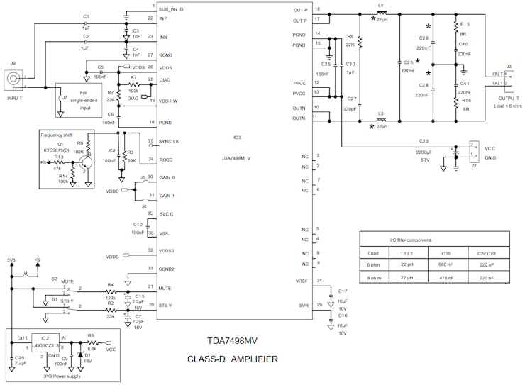
I got the reference of circuit and schematics from the official datasheet and it is my second attempt for the same amplifier and the previous one is not work completely for me. This time I make some changes in the circuit as stated in the datasheet. There are many options to set the overall gain, mute-standby, external voltage, and reference voltage of the PCB. I eliminate the use of complex circuitry and modified the voltage regulation section.
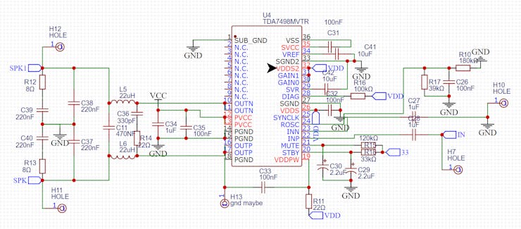
You can also pair the two device if stereo mode is recommended. And due to class D operation at the output of amplifier we need a powerful filtering section. Which can handle the load of 100w speaker. The real output of class D is not a analog signal but a varying PWM signal of high frequency which is filter to look like the original one by using LC filters.
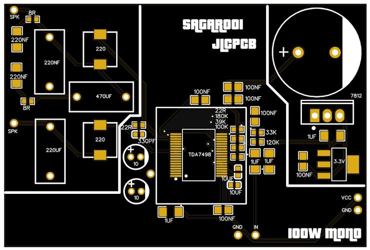
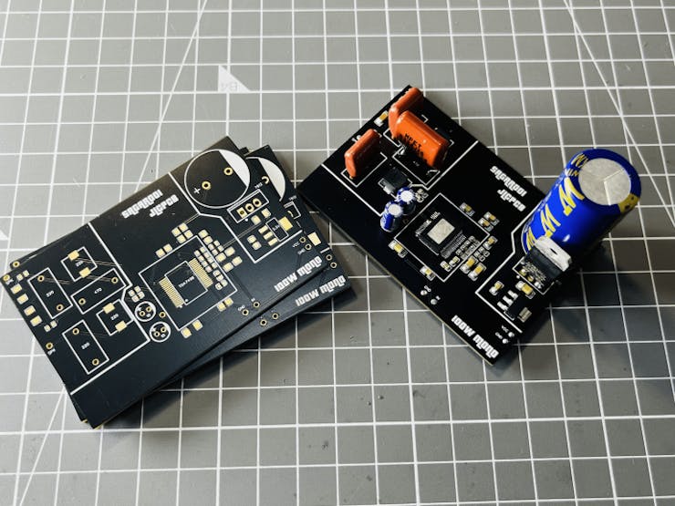
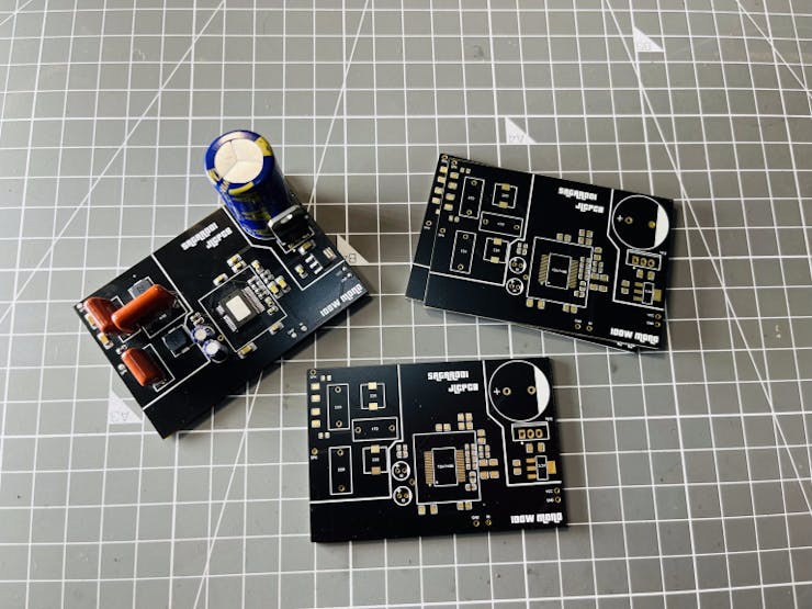
PCB designs and Gerber files:
In the amplifiers the common problem is of noise and humming. This may come due to any external power line fluctuation or may be due to any damaged and non-specified component. To keep the noise as low as possible there are few design consideration you should keep in mind.

Keep all the power lines away from the input signal tracks. And make sure to cover the whole PCB with GND net copper area. Keep all the ceramic capacitor away from the main IC they may produce oscillations. Use power line filtration capacitor at different places in the PCB plane.

If you want to use the same designs as mine then download the Gerber and SMT assembly files from here. You can upload these files to JLCPCB and order for the same PCB in just $2 for 5pcs. And SMT assembly service is starting from just $8 which in a total may cost $50 including assembly and components cost.
Hand assembly:
If you want to assemble the PCB by hand then the only solution is to use Stencil with it. Because there are too many small components and for even flow of solder paste stencil is required. JLCPCB is the one stop solution of all of your prototyping needs, you can explore the services like: PCB assembly (PCBA), Stencil, 3D printing services and multilayer ultra-precision PCB.
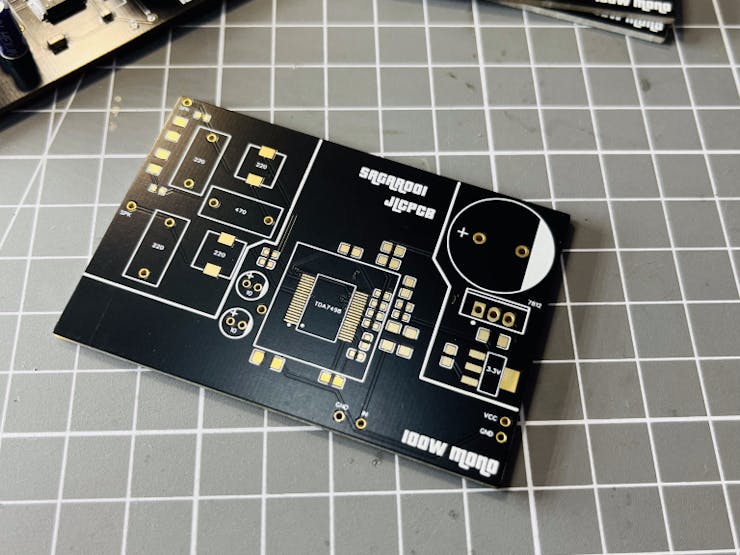
I use the same method I have all the components lane around and I used stencil with the PCB. Then I solder the PCB on a hot plate. In the PCB I used FR4 material, ENIG finishing and black colour with 1.6mm thickness.
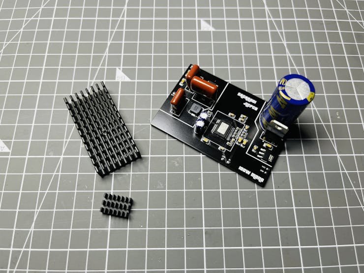
Heatsink and power SMPS:
This is class D IC which can be operated very efficiently on low voltage easily without any power dissipation. but for high output like 100watts, an external cooling system is required. Either you can use a small heatsink with small CPU fan or a little big heatsink. This will increase the overall stability and prevent any short circuit in the IC.
And for the power supply linear power supplies (Transformer with rectifier) is not recommended due to high ripple factor. Use any single power SMPS power supply which can supply at least 5amps at 24volts.
Working and performance of amplifier:
I paired the amplifier with a Bluetooth and hooked up the power supply. This time my circuit is working very well. In future I may improve the circuit components like instead of SMT filtering circuit I can use Trough hole components. Which also reduce the overall noise factor. The amplifier is fully silent when there is no input and it can handle a 100w subwoofer very well. You can see all the performance in the video given above.